The Path to Miniaturization: PCB Connectors for Compact Applications
In the fast-evolving world of electronics, the trend toward miniaturization is not just a passing phase. The compact innovations today may become tomorrow’s standard. The market drive towards smaller, more space-efficient devices bring significant challenges for engineers, particularly in the realm of Printed Circuit Board (PCB) connector design and manufacturing. As consumers demand sleeker, more compact devices, the industry is tasked with producing miniature PCB connectors that maintain, if not surpass, the performance of their bulkier predecessors, in terms of both electrical functionality and mechanical resilience.
Thermal Challenges in Miniaturization
One of the most pressing issues in miniaturizing PCB connectors is thermal management. As components become more densely packed to fit into compact enclosures, the electrical resistance increases, leading to excessive heat generation. This is not just a problem of user comfort or device longevity; overheating is a critical concern that could undermine the performance of the circuit.
For better thermal qualities, Mill-Max designs subcomponents with low contact resistance, reducing the heat produced during operation. The selection of higher-temperature materials, along with mechanical design strategies, can vary throughout a single connector:
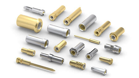
- Receptacles - Precision-stamped, multi-finger contact clips, inside each receptacle, boast an aggressive design which bites into the mating lead to form a gas-tight connection. For applications up to 150⁰ C, beryllium copper is an excellent material choice, while beryllium nickel operates up to 300⁰ C.
- Spring-loaded pins - For high temperature spring-loaded applications, stainless steel springs are the best choice. Mill-Max achieves extremely tight tolerances using precision turning of the components and accurately coiled springs that provide proper force to optimize biasing inside the pin and maximize the surface area at contact points.
- Contact finish - Gold plating on all contact surfaces is the final step in delivering low contact resistance.
Maintaining Mechanical Robustness in PCB Connectors
The reduction in size inherently brings into question the mechanical strength of PCB connectors. Miniaturized versions are not only more delicate due to their size but also must withstand the same mating cycles as their larger counterparts.
The contact clips achieve a longer lifecycle due to their multi-finger design, which can survive the same levels of shock and vibration as larger versions — according to IEC standards.
PCB Connector Space-Saving Techniques
In the face of spatial constraints and all the other physical challenges miniaturization brings, engineers employ a variety of tactics to shrink the footprint of PCB connectors.
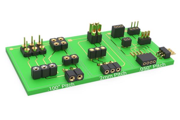
Reducing the pitch, or the pin-to-pin spacing, achieves a significant decrease in the overall size of the connector. Using staggered or interstitial spacing also helps to shrink the design without sacrificing performance. Over the years, Mill-Max has designed and manufactured ever-smaller contact clips for high-density receptacles to meet miniaturization challenges.
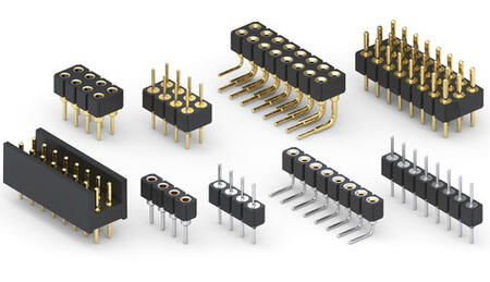
The use of carriers instead of traditional Single In-line Package (SIP) and Dual In-line Package (DIP) sockets has reduced height, while right-angle sockets, pin-headers, and spring-loaded connectors maximize the use of available space. Horizontal surface mounting and zero-profile receptacles can also be employed to further compact the design envelope.
A Neat Package
Mill-Max has optimized the packaging of many advanced pins and receptacles, utilizing tape-and-reel for automated placement onto PCBs. For large volumes, the tape-and-reel method drastically reduces the amount of time needed for board assembly and quality control.
Both surface-mount (SMT) and through-hole components are available for tape-and-reel packaging. Through-hole receptacles with an open bottom may incorporate a fibre plug, an organic paper solder barrier, which helps prevent solder from wicking up inside the receptacle into the contact area during reflow soldering operations. This allows for a good connection to be made when the mating lead is plugged in.
Leading the Way in PCB Connector Design
The Mill-Max objective is not just to keep pace with the trends but to actively shape the future of PCB connector design:
- Our latest line features spring-loaded pins, or POGO pins, for PCBs that offer reliable connectivity even when alignment is less than perfect.
- We introduced stacking interconnects that achieve various board-to-board heights between PCBs to take advantage of early engagement receptacles that work with low-profile nail head pins. These details help to minimize signal paths and reduce vertical profiles.
- Our latest offerings for miniaturization include a new line of 0.050”-pitch spring-loaded connectors with a 33% height reduction compared to previous versions.
Dedication Pays Dividends
Mill-Max's long commitment to innovative miniaturization has resulted in a diverse line of compact connector offerings. The efforts to deliver rugged, reliable, and miniaturized PCB connectors have been tested on real-world products in applications where performance and longevity are critical.
With a fully integrated production environment, Mill-Max maintains total control over the production process, ensuring quality from raw materials to the finished product. This holistic approach, combined with their commitment to providing customized solutions and unmatched customer support, ensures that Mill-Max remains a leader in PCB connector miniaturization.
Want to learn more? Contact our Technical Team today.


